The newest generation of transistor designs are the Gate All Around (GAA) transistors. It is designed to replace the FinFET in advanced semiconductor manufacturing, particularly at 2 nm, 3 nm, and beyond. The main function of transistors is switching to control the flow of electrical current or for amplification. In this article we are going to explain the Gate All Around Transistor. These transistors are called GAA for short.
Key Features and Functions of gate all around transistor
The main, or key, functions of Gate All Around Transistors are
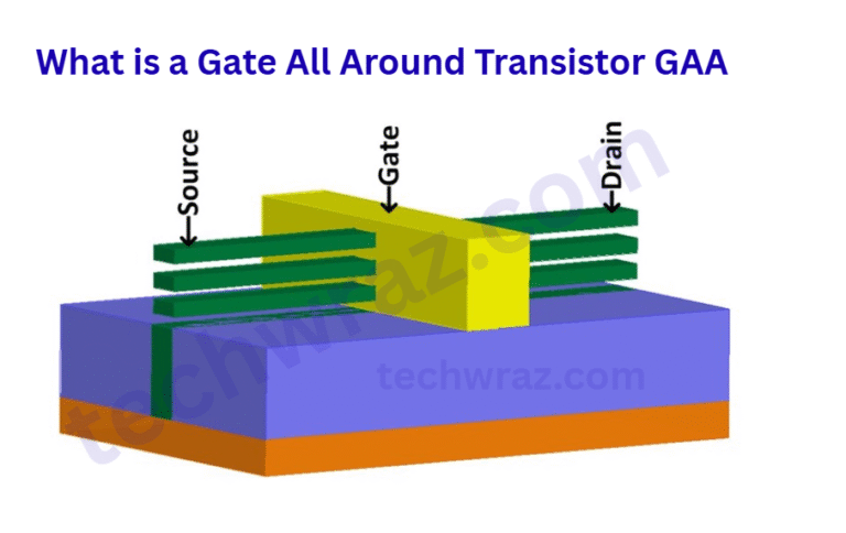
- Gate Control: The FinFET gate surrounds the conductive channel on only three sides, but the GAA design features a gate that completely wraps around all four sides of the channel.
- Channel Structure: The channel is often built using nanowires or nanosheets stacked horizontally or vertically, which are tiny wires or sheets of silicon.
- Superior Electrostatic Control: The gate exerts maximum electrostatic control for the flow of current because it wraps around all four sides. This feature is the best feature of the gate all-around transistor, or GAA.
How will gate-all-around transistors change our daily life?
Gate-All-Around (GAA) transistors, while a fundamental technological component, will not be something you directly interact with. Instead, their impact on daily life will be realized through the superior performance, efficiency, and capabilities of the electronic devices they power.
GAA transistors become crucial because they allow semiconductor manufacturing to continue the path of miniaturization. This is significantly improving power and performance metrics.
Here is how GAA transistors are expected to change or improve your daily life:
Primary Benefits of GAA Over FinFET
1. Superior Electrostatic Control
| Feature | Gate-All-Around (GAA) | FinFET | Benefit over FinFET |
| Gate-Channel Contact | 4 sides (The gate completely wraps the channel) | 3 sides (The gate wraps the sides and top of the fin) | Complete 360-degree control of the current flow. |
| Result | Provides the ultimate solution for carrier control in ultra-scaled transistors. | Control diminishes as channel width scales down. |
2. Reduced Leakage Current and Power Consumption
| GAA Benefit | Explanation | Daily Life Impact |
| Reduced Leakage ($I_{off}$) | With the gate fully surrounding the channel, the electrostatic field is much stronger and uniform. This allows the transistor to be “off” more effectively, minimizing the unwanted residual current flow. | Significantly better battery life for mobile devices (smartphones, laptops, and wearables). |
| Lower Operating Voltage ($V_{dd}$) | The improved control allows the transistor to switch reliably at a lower operational voltage. | Lower power consumption means less heat generation and better energy efficiency overall. |
Enhanced Performance and Scalability
| GAA Benefit | Explanation | Daily Life Impact |
| Higher Drive Current ($I_{on}$) | GAA structures (like nanosheets) offer a greater effective channel width in the same footprint. This allows more current to flow when the transistor is “on.” | Faster chip performance for tasks like gaming, AI processing, and complex computations. |
| Better Density Scaling | The nanosheet structure of GAA allows for vertical stacking of multiple channels. This means more active transistor area can be packed into the same chip footprint. | Enables the industry to continue Moore’s Law (more transistors per chip), leading to smaller, yet more powerful processors (e.g., at 2nm). |
| Design Flexibility | The width of the nanosheets can be tuned by the chip designer. | Allows for optimization: wider nanosheets for high-performance cores, and narrower nanosheets for low-power, high-efficiency cores on the same chip. |
Example of gate all around transistor (GAA)
- Samsung’s MBCFET™
- Intel’s RibbonFET™
- Nanowire GAA Transistors
- Forksheet FET (FSFET)
Planar FET vs FinFET vs GAAFET vs MBFET
The different among Planner FET, FinFET, GAAFET, and MBFET are shown in the diagram given below
You May Also Like
- Difference between BC547 and BC557 Transistor
- BC547 transistor pinout Datasheet
- C945 Transistor Pinout Datasheet
- Solar drone with wingspan wider than jumbo jet could fly for months
- Change the Direction of a DC Motor
- 12-volt battery level indicator
- An Introduction To Arduino
- The Future of Passwords: Are Biometrics and Passkeys the Solution?